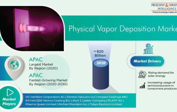
Physical vapor deposition is a widely utilized technology for thin films and surface coatings fabrication. The wide industrial application of the PVD involves various methods such as producing coatings with superior properties. The technological developments in nanoscience have resulted in the wide usage of this technology for the fabrication of layers with desired microstructure and properties.
Physical vapor deposition is a process that involves the transfer of material from the condensed phase to the vapor phase, and then back to the thin film condensed phase. Evaporation and sputtering are widely used processes of physical vapor deposition.
The physical vapor deposition involves sputtering or evaporation of different components for vapor phase production, supersaturation of the vapor phase in an inert atmosphere to facilitate metal nanoparticles' condensation, and nanocomposite consolidation by thermal treatment.
The cathodic arc deposition is also known as vacuum arc deposition. The high deposition of energy of the condensing atoms increases the utilization of the CAD processes essential for the growth of the film to facilitate adhesion and disrupt columnar growth. These energies rely on material dependence and range between 25 to 55 eV for iron and carbon respectively. Moreover, these energies rely on materials for high-quality film growth. It involves energies ranging from 25 to 100 eV for required activation of surface atom displacements, along with maintenance of good crystallinity.
Download sample pages of this report: https://www.psmarketresearch.com/market-analysis/physical-vapor-deposition-pvd-market/report-sample
The electron beam deposition involves utilizing electron beams for generating electron sources in a vacuum for evaporant material irradiation, along with heating and evaporating to generate a thin layer of evaporated materials, such as a lens or substrate. The deflection-type electron source is utilized in a wide range of fields, while direct-type electron sources are high powered, and facilitates quick evaporation. It is also used for deposition onto long films and large area substrates.
Sputter deposition can be defined as a physical vapor deposition method for depositing thin films. It involves sputtering the material from the target and further depositing it on the substrate. It is an important technique for CaP coatings preparation on polymeric or metallic substrates. It involves bombarding the Argon or Nitrogen plasma on the CaP target. The substrates are placed at a suitable distance in front of the target. The sputter deposition is quite similar to the plasma spraying. The positive ions of the plasma gas hit the target with the application of bias voltage on substrate holders. It also erupts the CaP that is further deposited on the substrates.
The properties of the deposited CaP coatings can be controlled by optimizing the sputter deposition conditions. It includes substrate distance target, target current, deposition time, bias voltage, and pressure inside the chamber. Moreover, the sputtering can be carried out by utilizing RF sputtering, ion-assisted deposition, magnetron sputtering, or pulsed-layer deposition.
The sputter deposition facilitates the high-quality epitaxial superlattices and thin films of complex oxides at an extremely low cost compared to others. It also facilitates the high quality of oxide films led by the interest in a specific class of complex oxide materials and results in scientific progress.
Sputter deposition is highly preferred for thin film applications where density, purity, and stoichiometry hold a prominent position for the functionality of the films. The evolutionary advances and refinements that facilitate sputter deposition tooling and processes for rough cadence continue proceeding with semiconductor industry technology nodes.
Therefore, the scientific progress led by the decline in cost of high quality oxide films facilitated by the sputter deposition boosts the industry.